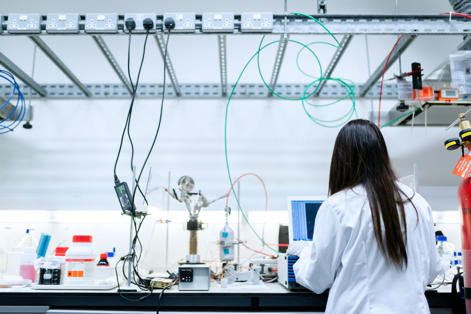
The Telangana government has taken a pioneering step in strengthening India's semiconductor manufacturing ecosystem by launching the nation's first Chemical Mechanical Planarization (CMP) pad technology center in Hyderabad. This initiative represents a crucial development in the country's journey toward self-reliance in semiconductor production and advanced electronics manufacturing.
Understanding CMP Technology
Chemical Mechanical Planarization is a critical process in semiconductor wafer fabrication. During chip manufacturing, multiple layers of materials are deposited on silicon wafers to create integrated circuits. CMP technology ensures these layers are perfectly flat and smooth by combining chemical etching with mechanical polishing. The CMP pads are consumable components that play an essential role in this polishing process, directly impacting the quality and performance of semiconductor chips.
The technology is indispensable in producing modern microprocessors, memory chips, and other semiconductor devices found in smartphones, computers, automobiles, and virtually all electronic equipment.
Strategic Importance for India
India currently imports nearly all specialized semiconductor manufacturing materials, including CMP pads, primarily from countries like the United States, Japan, and South Korea. This dependency creates supply chain vulnerabilities and increases production costs for domestic semiconductor facilities.
The establishment of this technology center aligns with India's broader semiconductor mission and the government's push for Atmanirbhar Bharat (self-reliant India) in critical technology sectors. By developing indigenous CMP pad manufacturing capabilities, India can:
- Reduce import bills and foreign exchange outflows
- Strengthen supply chain resilience for semiconductor fabrication
- Support the growing domestic electronics manufacturing industry
- Create specialized employment opportunities in advanced materials science
- Position India as a competitive player in the global semiconductor supply chain
Telangana's Technology Leadership
Hyderabad has emerged as a major technology and innovation hub, hosting numerous global technology companies, research institutions, and startups. The city's ecosystem includes established semiconductor design centers, electronics manufacturing facilities, and academic institutions with strong engineering programs.
The state government has actively promoted Hyderabad as a destination for semiconductor and electronics manufacturing investments. This CMP pad technology center adds to existing initiatives and infrastructure, creating a more comprehensive semiconductor ecosystem within the state.
Expected Impact on Manufacturing Ecosystem
The technology center is expected to serve multiple functions beyond just CMP pad production. It will likely focus on:
- Research and development of advanced CMP pad materials and designs
- Technology transfer and commercialization partnerships with industry
- Training programs for engineers and technicians in semiconductor manufacturing processes
- Quality testing and certification of CMP pads for various applications
- Collaboration with upcoming semiconductor fabrication facilities in India
Several semiconductor fabrication projects are in various stages of planning and approval across India. Having domestic access to critical consumables like CMP pads will reduce operational costs and improve supply chain predictability for these facilities.
Challenges and Opportunities
Developing competitive CMP pad technology involves significant technical challenges. The pads must meet extremely stringent specifications for uniformity, durability, and performance. They must work effectively with various materials including silicon dioxide, silicon nitride, and metals like copper and tungsten.
International manufacturers have decades of experience and established supply relationships with global semiconductor fabs. The Indian center will need to demonstrate comparable quality and reliability to gain market acceptance, even domestically.
However, the growing global demand for semiconductors, coupled with increasing emphasis on supply chain diversification following recent global chip shortages, creates opportunities for new suppliers who can meet quality standards.
Future Prospects
The center represents an important first step, but scaling up to commercial production and achieving cost competitiveness will require sustained investment, skilled workforce development, and close collaboration between government, academia, and industry.
Success in CMP pad technology could pave the way for India to develop other semiconductor materials and consumables, gradually building a complete domestic supply chain for chip manufacturing. This would significantly enhance India's position in the global semiconductor industry and support the country's ambitions in electronics manufacturing and export.
The initiative demonstrates how targeted investments in specialized technology niches can create strategic advantages and contribute to broader industrial development goals.